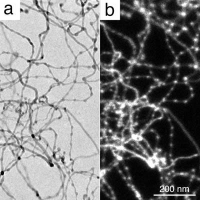
TEM image of the chains of silicon nanocrystallites formed by (a) elastically scattered electrons and (b) electrons which excited a silicon bulk plasmon.
go to Kohno Group Home
We have fabricated chains of silicon nanocrystallites: silicon nanocrystallites are arrayed periodically in one-dimensional order. In Figure (a), we show a TEM image of the chains. Figure (b) is an energy-filtered TEM image of the same region formed by electrons which had exited a silicon volume plasmon, and the bright regions correspond to the silicon crystallites. The background is a vacuum. A silicon nanocrystallite exists in the center of each knot, which is covered and connected to the neighboring crystallites by amorphous material which is presumably silica. The spacing between and the diameter of nanocrystallites in a chain are almost uniform. The chains were synthesized by a thermal treatment of a gold-coated silicon substrate. Silicon nanowires were also grown. Both chains and wires should have been grown via the well-known vapor-liquid-solid (VLS) mechanism which is a typical growth mechanism of whiskers. Numerous semiconductor nanostructures have been grown so far aiming drastic changes in the optical and electrical properties due to the quantum confinement effect, however, it is remarkable that our chains were grown via a self-organized process. In addition to the physical interest, the chain of silicon nanocrystallites is in expectation of application to a new functional material.
TEM image of the chains of silicon nanocrystallites formed by (a) elastically scattered electrons and (b) electrons which excited a silicon bulk plasmon.
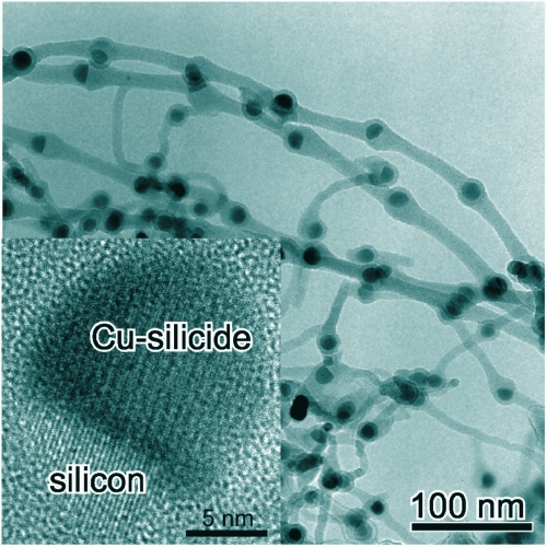 Cu-silicide nanochains
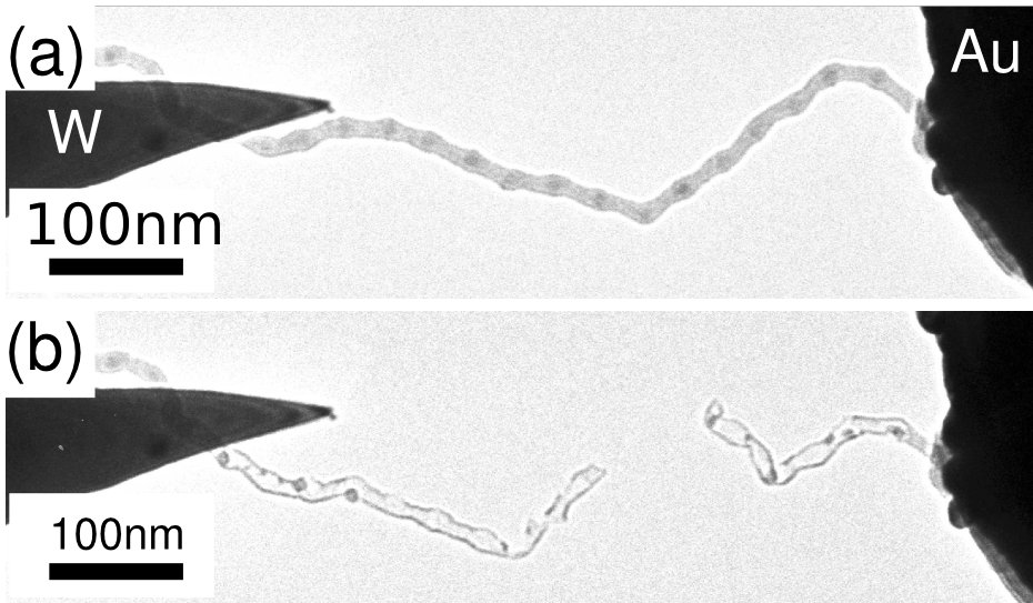 Transforming a silicon nanochain into a carbon nanotube